Last week, a long-standing client—a contract manufacturer in Silicon Valley specializing in tier-one semiconductor components—sent us an urgent email. While machining the final, intricate fine grooves of a batch of high-purity graphite boats, they hit a wall. Microscopic chipping along the slot edges suddenly appeared, rendering the entire batch of expensive, semiconductor-grade workpieces complete scrap.
We see this exact nightmare far too often on the front lines of precision manufacturing. Graphite processing in the semiconductor sector is never a matter of ordinary machining; the demands for dimensional tolerances and material purity border on the obsessive. Yet, many shops still attempt to tackle these specialized materials using standard carbide tools, or ordinary diamond-coated tools with substandard adhesion. The result is always a spike in cutting forces, leading directly to thin-wall fractures and surface roughness (Ra) values that bust QC specifications.
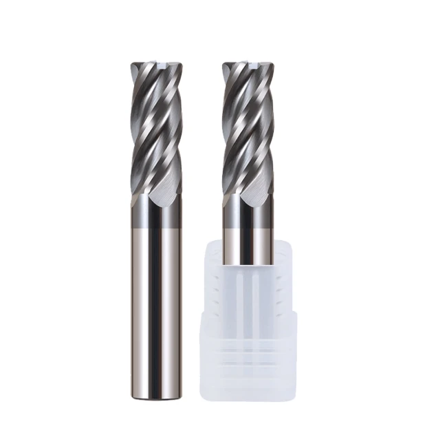
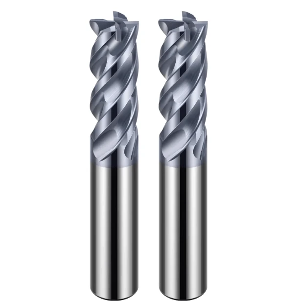
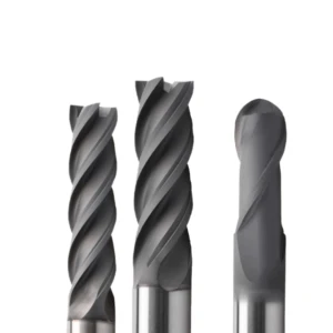
As a tool manufacturer with 15 years of hard-won shop floor experience, we know that semiconductor processing leaves zero room for guesswork. Achieving micron-level dimensional stability during high-speed milling hinges entirely on whether your end mills for graphite possess the exact core geometry and coating integrity required to withstand extreme abrasive wear.
In this guide, speaking engineer-to-engineer, we will bypass textbook theory to break down the mechanics of CVD coating delamination, edge preparation, and substrate formulation. We will explain why, as a primary manufacturer of china diamond coated end mills, we insist on controlling cobalt content down to a strict 0.1% variance. We will also look at the procurement side, helping you identify diamond coated end mill suppliers that offer a genuine technical moat to eliminate costly batch-to-batch downtime.
When faced with semiconductor-grade graphite—a material notorious for devouring cutting edges—is your workshop currently trapped in a costly loop of frequent tool changes and bleeding spindle efficiency?
The Rigorous Demands of the Semiconductor Industry for Graphite Components: Why Are Standard Diamond End Mills Insufficient?
Many operators harbor a common misconception: because graphite is soft to the touch, any standard diamond-coated tool can cut it. In the semiconductor realm, this logic fails immediately. High-purity isostatic graphite has an incredibly fine grain structure that acts like a micro-abrasive wheel against the tool edge. A standard diamond end mill designed for general carbon fibers lacks the specialized flute relief needed for sub-micron dust, causing rapid friction buildup and microscopic tearing on the workpiece.
We frequently remind our clients’ field engineers that the machining window for semiconductor components is unforgivingly narrow. Even a few microns of edge wear causes cutting resistance to rise exponentially, generating localized stress. This subsurface stress leads to workpiece warping or micro-fractures during subsequent high-temperature processes like epitaxial growth or plasma etching. Standard general-purpose tools simply cannot provide the sustained cutting rigidity these high-load setups demand.
From Graphite Boats to Etch Rings: Micron-Level Tolerances—The Ultimate Test for Diamond End Mill Cutting Tools
Among the core semiconductor components we supply, graphite boats, wafer carriers, and plasma etch rings present the most grueling challenges. These workpieces often feature hundreds of dense, narrow slots with wall thicknesses under 0.5 mm, while print tolerances demand control within ±5 microns. During continuous, 30-hour high-speed CNC cycles, even minor dimensional drift scraps the entire setup, placing brutal demands on the runout of diamond end mill cutting tools.
Through years of optimization, our team found that conventional tool paths leave minute step marks at the slot bottom that compromise structural integrity. To eliminate these deviations, both the dynamic balance and cutting-edge symmetry must undergo a specialized, automated grinding process. If the tool exhibits a radial runout of even 2 microns at 30,000 RPM, the resulting micro-resonance will instantly shatter fragile graphite teeth, which is why we utilize asymmetrical helix geometries.
Preventing Wafer Contamination: How We Strictly Control the Purity of Tool Body Substrates When Manufacturing End Mills for Graphite
In semiconductor manufacturing, material purity is just as critical as dimensional precision. For graphite components used in ion implantation or etching, a single ppm of metallic contamination (like copper, iron, or nickel) can ruin an entire wafer lot. Many shops fail to realize that secondary contamination often comes directly from the tool body; as the cutting edge wears, microscopic substrate particles rub directly into the porous graphite matrix. This is why our raw material vetting for end mills for graphite is uncompromised.
During the tungsten carbide sintering phase, we work closely with metallurgical labs to reconfigure the cobalt (Co) binder matrix and eliminate trace heavy metals. Our domestic production lines utilize specialized ultra-pure chemical cleaning and deionized water flushes to strip all surface residues post-grinding. This ensures that every tool delivered to our customers’ workshops is not only geometrically perfect but also chemically clean enough for sensitive cleanroom environments.
Case Study: An Analysis of a Semiconductor Graphite Disk Scrap Incident Caused by Tool Chipping
Last year, a prominent semiconductor equipment supplier in Munich reached out to us after scrapping a critical batch of MOCVD graphite base disks. They were using premium European off-the-shelf tools, but the micro-geometry featured an excessively sharp, fragile edge radius. After 14 hours of continuous machining, the tool encountered a section of high-density hard inclusions in the graphite, causing a microscopic chip on the primary cutting edge.
This tiny failure localized the cutting stress, changing the tool action from a clean shear to a brutal rub. The resulting force instantly fractured the delicate wall of a high-precision wafer pocket, scrapping a part valued at tens of thousands of dollars. We solved this by implementing our customized china diamond coated end mills, modifying the micro-hone radius and increasing coating adhesion layers, which stabilized the client’s final yield rate at over 99%.
Core Technology Analysis: Key Metrics for Extending the Lifespan of China-Made Diamond-Coated End Mills
For years, overseas machine shops held a stubborn stereotype: Chinese cutting tools offered great value but suffered from highly inconsistent operational lifespans. As a domestic manufacturer, let us be completely direct: this lifespan variability is not caused by substandard production machinery. Leading domestic factories now utilize top-tier, 5-axis grinding centers from world-class brands like Walter and DMG MORI. Instead, the real differentiator lies in the meticulous deconstruction of microscopic process parameters.
When machining highly abrasive semiconductor-grade materials, high-performance china diamond coated end mills are far more than just a standard carbide substrate with an off-the-shelf coating. True tool longevity requires a systematic synergy across multiple core metrics. We balance substrate decobaltization, nanoscale crystal growth control, and post-coat surface flatness to survive the brutal shop environment. To achieve this, we enforce three inviolable technical imperatives within our daily production workflow.
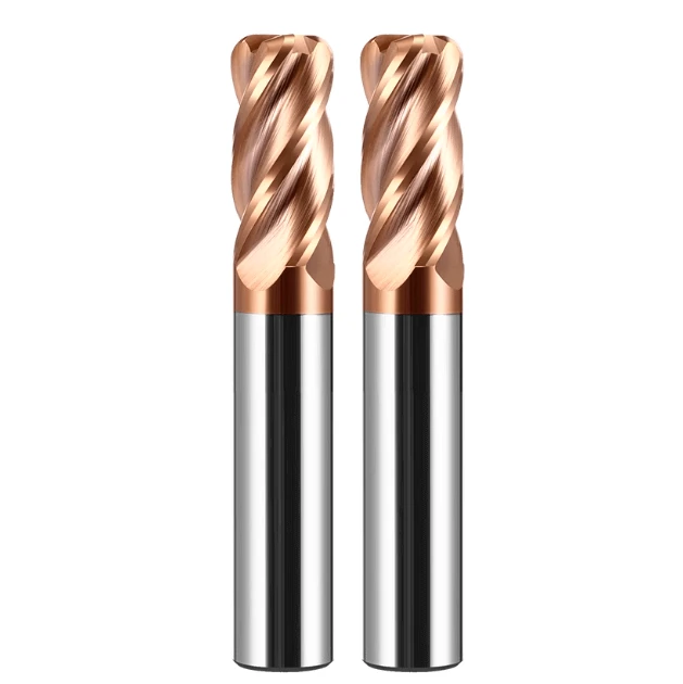
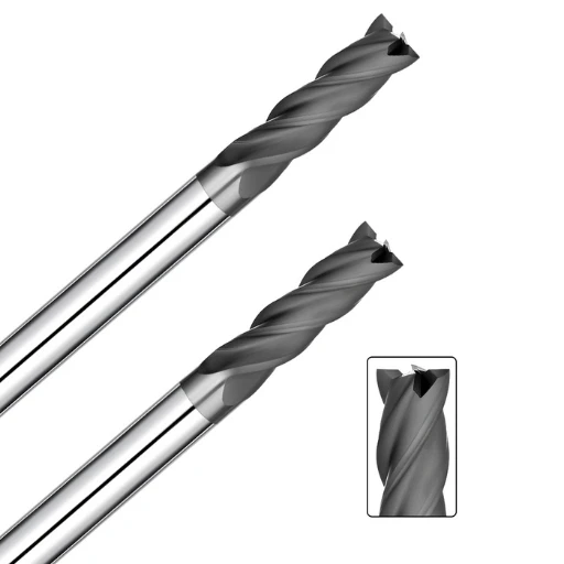
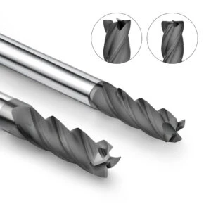
CVD Diamond Coating Adhesion: Practical Experience in Resolving Coating Delamination in Semiconductor Machining
In the graphite machining sector, the ultimate production nightmare is a protective coating that suddenly peels off the tool in large flakes. We diagnosed this exact issue for a British manufacturer milling miniature semiconductor fixtures using a competitor’s diamond end mill. On the rack, the tools looked flawless; under microscopic inspection, however, the primary diamond layer had completely detached from the carbide base. Once high-hardness graphite creates a microscopic void at the interface, delamination spreads instantly like a chain of falling dominoes.
To permanently cure this failure mode, we overhauled our chemical pre-treatment and decobaltification process. Cobalt is a necessary binder for cemented carbide, but during high-temperature vapor deposition, it acts as a catalyst that forces diamond back into soft graphite. Through a multi-stage chemical etching process, we precisely strip cobalt elements from the substrate surface to a depth of several microns. We then apply proprietary laser texturing to form microscopic “dovetail” interlocking structures, providing the mechanical anchoring strength needed to stop peeling under heavy radial forces.
The Art of Edge Preparation: Why We Insist on Specific Passivation Processes When Manufacturing Diamond-Coated End Mills
In conventional metal milling, machinists always pursue the sharpest edge possible to minimize shearing resistance. However, when manufacturing specialized diamond coated end mills, a razor-thin cutting edge is actually a liability. Many junior field engineers struggle to understand why we deliberately dull a newly ground, perfectly sharp edge before coating it. Our 15 years of manufacturing experience show that an untreated, razor-sharp edge creates a severe “tip effect” in the CVD reactor, causing diamond crystals to grow abnormally large and brittle.
To prevent immediate chipping on the first part, every tool we make undergoes a strict micro-honing passivation protocol. We bypass aggressive polishing wheels entirely, choosing micro-fluidic blasting and slurry-based lapping to hone the edge into a uniform, smooth “K-Land” profile. We control this edge radius within a tight tolerance of just a few microns. This precise geometry provides the structural backing needed to survive heavy cutting impacts while remaining sharp enough to prevent the tool from pushing and crushing fragile graphite structures.
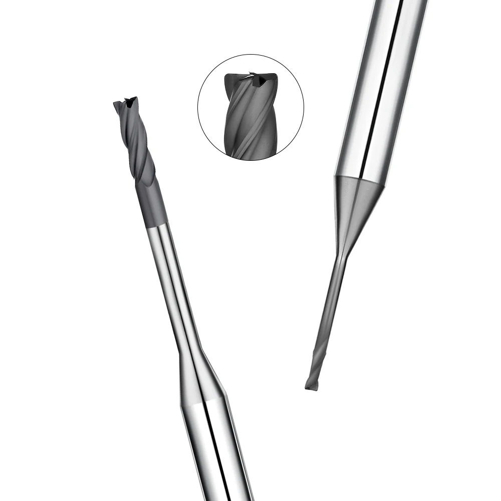
Flute Design and Dust Evacuation: Optimized Solutions for End Mills Dedicated to High-Purity Semiconductor Graphite
Milling semiconductor graphite is unique because the material never forms continuous, ribbon-like chips; it instantly pulverizes into an ultra-fine, abrasive powder. If this high-density dust is not evacuated immediately from the rotating helical flutes, it acts like a grinding wheel that erodes the tool’s flank face. Conventional flute designs lack the necessary volumetric space, causing dust to compress and pack tightly within the channels. This chip packing spikes cutting temperatures and quickly snaps the delicate shanks of specialized end mills for graphite.
To eliminate evacuation bottlenecks in deep-cavity work, we abandoned standard general-purpose flute shapes. Our specialized tools feature a modified parabolic curvature on both the rake face and the chip flutes, paired with an asymmetrical helix angle. Furthermore, because a high-quality CVD layer adds 10 to 15 microns of physical thickness, it naturally alters the tool’s final geometry. We proactively calculate this coating allowance during the initial grinding phase, ensuring dust is drawn out the instant it forms to protect the workpiece finish.
Engineer’s Selection Guide: How to Identify Reliable Suppliers of Diamond-Coated End Mills
Overseas procurement managers are routinely overwhelmed by glossy marketing brochures making identical performance claims. However, as fellow engineers who live on the shop floor, we know that selecting the right vendor does more than protect your tooling budget—it saves your delivery schedule. Machining high-purity graphite leaves absolutely zero margin for error. While many general tool companies add graphite items to their catalogs, they merely mass-produce standard shapes and lack the deep materials expertise required to vet reliable diamond coated end mill suppliers.
Through our years of handling OEM orders for Western buyers, we found that true supplier competency shows up in non-standard customization and pre-sales technical support. Semiconductor operations need a technical partner who speaks the language of the shop floor, understands spindle rigidity, and respects vacuum extraction limits. If a potential vendor gives vague answers regarding tight micro-tolerances or specific graphite grades like Poco or SGL, their tools will likely fail you. Working with an unverified vendor often leads to frequent downtime and unpredictable tool wear during mass production.
Technical Support Capabilities: Can a Qualified Supplier Adjust Tool Geometry Parameters to Suit Your Specific Semiconductor Machining Conditions?
In actual production, even identical semiconductor parts present entirely different machining behaviors based on your machine tool setup and dust extraction power. To prevent moisture-induced graphite expansion and cleanroom contamination, some shops run entirely dry with chilled air lines. Other shops rely on high-pressure air blast systems to violently purge the cutting envelope. If a supplier only hands you a standard catalog diamond end mill cutting tools, you will never achieve maximum efficiency across these two operational extremes.
As an active technical support team, we know exactly how much a minor geometry tweak changes dust flow. In dry, enclosed setups where static electricity makes graphite dust adhere to the tool, we widen the secondary relief angle to reduce friction. For high-pressure air blasting, we optimize the helix angle and polish the flute surface to slickly eject particles into the vacuum stream. A qualified supplier must be willing to modify your next batch based on actual spindle load data, rather than forcing you to modify your process.
Batch Consistency: How We—as a Manufacturer of Diamond-Coated End Mills—Ensure the Uniformity of Every Single Tool Through Fully Automated Inspection Equipment
For dedicated semiconductor component foundries, nothing is more frustrating than a tool batch where the first mill runs for 20 hours but the second snaps in 5. This tool-life variance completely destroys a shop’s ability to run safe, unattended lights-out shifts. As a premium manufacturer of china diamond coated end mills, we know that international trust relies entirely on batch consistency. To eliminate human error from the grinding equation, we implemented a completely closed-loop automated quality control chain across our entire facility.
We integrated automated German Coordinate Measuring Machines (CMMs) and non-contact optical multi-sensor systems directly into our production workflow. From sorting carbide blanks for raw roundness to inspecting finished edges post-grinding, every tool undergoes 100% automated verification with real-time wheel wear compensation. For the critical CVD phase, we deploy in-situ thickness monitors and laser scratch testers to verify coating uniformity. This automated approach ensures that every tool delivered to your shop maintains a micron-level tolerance window on runout and passivation.
ROI Analysis of Cost and Efficiency: Why Semiconductor Clients Prefer Diamond-Coated End Mill Suppliers with Strong R&D Backgrounds
Modern purchasing strategies in the semiconductor sector have shifted away from the raw purchase price toward a strict “Cost Per Part” calculation. A cheap tool that suffers from a short lifespan causes frequent machine stops, constant re-touching, and risks scrapping an entire multi-thousand-dollar graphite chuck. This hidden operational cost quickly eclipses any upfront savings. This is why tier-one manufacturing firms in the US and Europe audit their supply chains to favor specialized diamond coated end mill suppliers with dedicated materials laboratories.
An R&D-driven supplier delivers continuous process improvements that directly protect your profit margins. When our lab refines a carbide substrate’s grain structure down to the ultra-fine sub-micron level, or adjusts gas dynamics to increase coating density, your shop reaps the rewards. In real-world terms, these engineering updates translate to a 15% increase in spindle feed rates and a 30% drop in total tool consumption. This deep engineering support gives you the technical edge needed to win tough contracts and maintain profitability on ultra-pure graphite.
Common Issues and Machine Tuning Strategies in Semiconductor Graphite Machining
Once you master coating adhesion and secure reliable vendors, your ultimate success comes down to your CNC control panel. As engineers with over a decade of frontline tuning experience, we know that poor cutting parameters or bad toolpaths will ruin the best tooling. Semiconductor graphite machining requires a precise equilibrium between cutting forces and brittle material removal at high spindle speeds. In our daily technical support, we frequently see premium tools suffer premature wear or catastrophic breakage simply because process parameters were rigidly applied without adaptation.
If you are currently struggling with deep-cavity corner clearing or ultra-precision mating surfaces, we encourage you to critically re-evaluate your tuning strategies. Graphite’s lack of ductility means that even tiny micro-vibrations during high-speed cutting amplify into severe surface defects. By meticulously deconstructing spindle speed, feed per tooth, and depth of cut, we have formulated a baseline workshop methodology. This practical troubleshooting guide helps machinists unlock the true performance of their tools by making precise, real-time adjustments during actual live machining operations.
Eliminating Thin-Wall Vibration: Optimizing the Speed-to-Feed Ratio for Micro-Diameter Diamond End Mills When Machining Precision Grids
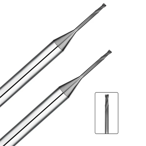
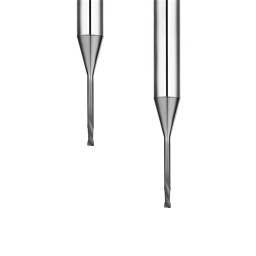
When machining semiconductor wafer carriers or fluid valves, dense, thin-walled grid structures are highly susceptible to tool deflection and edge chipping. If you are using a micro-diameter diamond end mill under 2 mm to slot high-aspect-ratio geometries, abandon traditional deep-cut, slow-feed strategies. Switch instead to a high-speed, light-cut, fast-feed approach. Lowering the feed rate on a fragile wall actually increases tool dwell time and frictional contact, which triggers destructive resonant vibration.
Based on our field experience, running your spindle between 24,000 and 30,000 RPM with a brisk feed of 0.01 to 0.03 mm per tooth shears the material before stress waves propagate to the thin-wall root. If you notice visible burrs or micro-chipping along the slot floor during setup, immediately check your radial runout. In these ultra-light setups, a runout exceeding 3 microns disrupts the per-tooth load balance and instantly shatters the fragile graphite teeth.
Surface Roughness (Ra) Control: Achieving Polish-Free Surface Finishes with High-Performance Diamond End Mills
Semiconductor epitaxial wafers demand stringent surface finishes, often requiring an $Ra$ under 0.4 microns or a mirror finish to prevent particle entrapment. If you are constantly tweaking your post-machining polishing process to eliminate a hazy finish, look closely at your final finishing stage. Evaluate how your diamond end mill cutting tools behave during shallow axial passes. While graphite removes via micro-particle detachment, a stable scraping action can achieve a high-gloss finish directly on the machine.
For this final finishing stage, we highly recommend using a premium corner-radius or large ball-nose cutter to minimize residual cusp height. Keep your axial depth of cut (Ap) strictly limited to approximately 0.05 mm. If the workpiece looks bright and lustrous in one direction but dull and matte in another, ditch parallel paths for contour-following or 3D spiral toolpaths. This continuous climb-milling approach suppresses microscopic surface tearing to hit high-cleanliness roughness specs without manual polishing.
Tool Pre-warning Mechanism: Our Recommendations for Engineers on Setting Reasonable Tool Replacement Frequencies When Machining Semiconductor Graphite Components
In high-volume semiconductor component manufacturing, trying to squeeze every last minute of life out of a cutting edge always comes at a steep cost. If you run unattended night shifts or process high-value, specialized graphite boats, you must establish a rigid tool replacement pre-warning mechanism. Relying on operators to visually check for wear or waiting for audible anomalies is a recipe for disaster. In a semiconductor-grade environment, hearing a change in pitch usually means a batch of scrap has already been produced.
We recommend documenting the exact cutting volume or linear travel distance achieved by new end mills for graphite before the surface finish degrades. For example, if a tool model shows an average safe lifespan of 18 hours on a specific graphite grade, set your machine’s internal tool-life counter to 14 or 15 hours. This tiered safety redundancy forces a tool change before microscopic coating spalling begins. This keeps your scrap rate locked at a negligible level while ensuring your spindle operates under optimal, low-stress conditions.
Every workshop differs in machine rigidity, vacuum extraction power, and raw material grades; therefore, no single set of parameters fits all production lines. If you are currently encountering persistent resonance, edge chipping, or abnormal tool wear in your semiconductor setup, please reach out to our team. We are ready to review your specific on-site conditions, 2D/3D product drawings, and graphite material grades. Let’s collaborate to engineer a customized tool geometry and process optimization plan perfectly tailored to your workshop’s existing capabilities.